Antumbra KLIK: Build Diary #23

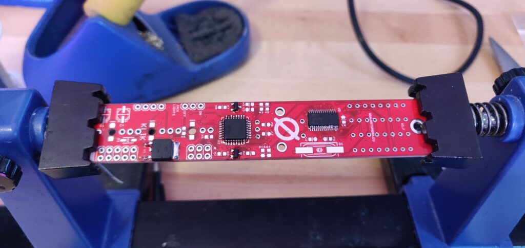
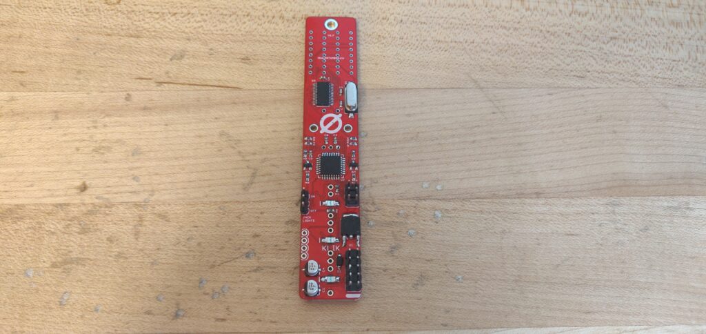
It’s Sunday, and you know that means I’m legally obligated to provide some bloggo’du’music, so this week we are talking about Antumbra’s KLIK.

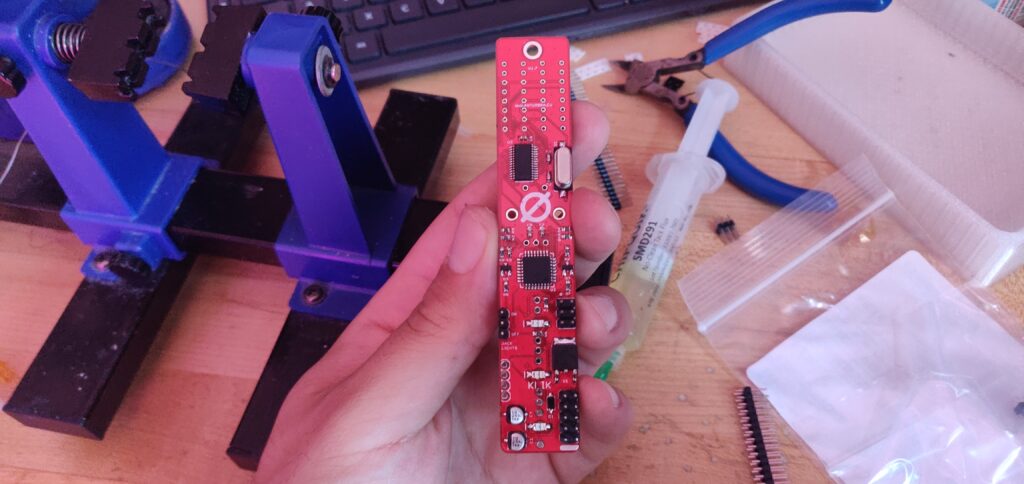
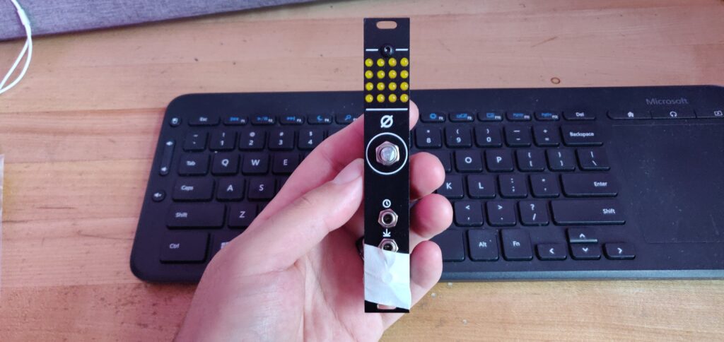
KLIK be a trigger sequencer from Antumbra, and it is rather gnarly. Don’t take my word for it, take it from KLIK’s creator:

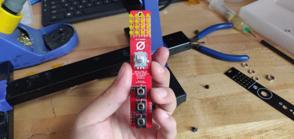
KLIK is a small and simple 16 step trigger sequencer with an intuitive interface. It features a 4×4 LED matrix as the interface which is easily navigated with the encoder and it’s pushbutton.

This interface enables a simple menu, which allows you to access several features, like euclidean mode, sequence length, direction, and different ways of random pattern generation.


Triggered random pattern generation is available through the reset jack.

Doesn’t that sound lovely? I was commissioned to build two of these, and the gentlemen who commissioned the build also grabbed a PCB/Panel combo for me. What a sweetheart! He must have known I loved Antumbra. After all, we’ve built the CARA, ATOM, and KNIT, just to name a few. Click the names if you want to see those builds! 

Any-who, let’s get this puppy on the bench.

But Steve, Isn't There a Great Build Guide Already Available?

Good point pushy heading. Before I get into showing my cute little build, check out the build guide Antumbra put together. It’s great for part placement, and very well illustrated. You can grab it here (click me).

My only disagreement is with step 14. I would personally solder the 3 SMD LEDs (step 15) and then solder those electrolytic caps. And that’s what I did on my three builds, made it much easier to pop the SMD LEDs in there.

Annnnyyways.

KLIK PCB on a PCB holder with the ICs soldered
Just followin' the build guide captain.

The LED driver is probably the toughest thing to solder on this bad boy. The Atmega 328P is a great chip to start with if you’ve never hand soldered these QFP packaged chips. Although, with the LED driver on this board, the KLIK might be a tough place to start. Definitely not insurmountable, but I would send first timers toward something like the Mutable Instrument Branches.

A photo of the complete PCB being held
A nice smoooth build thanks to a nice smoooth guide.

Flashing - Everyone's Favourite Part

This is probably the most tedious part of the build. I bought my chips off eBay, so they needed to be flashed. Thankfully the eBay chips were legitimate, which is always a concern, and after stumbling on the v1.5 build guide for KLIK, things became quite simple.

But before we get there, we gotta revisit the cute little Arduino ISP programmer I used to flash the chip.

An image showing an arduino, a cable, and the PCB, items needed for flashing.

I could never get the AVR ISP MKII to work properly. I have one, and tried everything under the sun to get it working. I gave up on that tool, and moved onto my old friend the Arduino. I followed the directions from a lovely little blog called hardwarefun.com. The long and short of it really come down to the following:

1. Flash the Arduino using the IDE with the ArduinoISP sketch.

Goto File -> Examples -> Arduino ISP


2. Hook up your Arduino as follows:

  • Arduino Pin 13 to SCK
  • Arduino Pin 12 to MISO
  • Arduino Pin 11 to MOSI
  • Arduino Pin 10 to RESET
  • Arduino 5+ to Vcc
  • Arduino Gnd to Gnd
  • 10 uF capacitor between Arduino Reset Pin and Gnd Pin (+ve leg of capacitor should go to Reset pin)

3. You’ve got an Arduino ISP programmer!

Arduino as an ISP Programmer
I think I've mentioned this in a prior post... but it's too cute not to post again!

Let’s do it then!

Back to the V1.5 guide. I was trying to figure out what values to use to set the fuses, and after a long night of KLIKing around on the internet (sorry, couldn’t help myself), I saw the V1.5 build guide was a little different. You can see the whole thing here, but I was only interested in this portion:

Guide describing how to flash the chip, pge 13
Ignore the first part, download the 1.7 firmware from the Anutmbra website (linked below as well)

So, with these directions and my new found confidence, I fired up AVRDUDESS (which I just recently discovered is a cool GUI for the avrdude program, NEAT) and got to flashin’.

I programmed 3 of these with the following settings, so I am confident you can too! YOU CAN DO THIS!

AVRDUDESS Screenshot
Done and done! But WAIT. Isn't that an error at the end?!

You may have noticed the error at the end of the AVRDUDE command that the GUI runs. But don’t fret my sweet little blog reader. You can either trust me that it is fine, or you can read the following quote from world wide web:

There was a change in how AVRdude treats unused fusebits – they used to be treated as 0, now they are treated as 1. So 0xFD is now the same as 0x05 used to be.

RELLLAXXX and let’s get KLIKKKIN.

Antumbra KLIK PCB that has been flashed
Ah it looks so differen't when it's flashed.

Hardware Time + A Small Catastrophe

Now that we’re all flashed up, time to throw the hardware on there! As always, put it all on the board, and don’t solder until you’ve got the panel attached everything lined up properly.

One thing to note here, the encoder does sit very far away from the PCB, this is normal.

An image showing how far away the encoder needs to mounted
Definitely has some distance to it.

Pull the encoder as far back from the PCB as you can without loosing contact. It’s OK if the pins aren’t sticking through the PCB. Just soak that hole down with solder and double check the pins afterwards.

Antumbra KLIK with the Hardware Attached
Looking good! But what sort of catastrophe could strike this late in the game?

So that was all good and fun. And I decided to re-rack some of my modules (I’m downsizing my Euro setup currently in anticipation of the new Buchla additions to the family) and we had a little “whoopsies”.

I didn’t connect the power cables first, and ended up reaching around back of the rack and kinda feeling my way around to get this one plugged in…

…turns out I plugged the power cable half into the ISP connector, and shot 12volts of sweet sweet juice directly into the microprocessor. That’s what we call a “whoopsies”. 

So now it is sitting on my bench waiting for a day where I have the patience to replace the MCU. Oh well! This is the twisted web we weave, after all.

A photo of a completed ANTUMBRA KLIK module with tape around the bottom output

The End, C'est Fini

It’s a fantastic module. There are all sorts of modes outside of the standard 16 step trigger sequencing function. And at 4hp it truly is something I will be fixing and returning to my rack ASAP.

With that all said, thanks for poking around again for the week. It is always much appreciated. Hope your last week was a beauty, and this one is even more beauty-ey.

Keep it samesies out there folks!

Quick Links

Antumbra KLIK Main Site Page – Main page for the module. Lists details and has all the links you could ever want or need.

V1.7 PCB Build Guide

V1.5 PCB Build Guide (includes flashing directions that work for V1.7)

Mouser BOM – Found on the Antumbra site, I don’t want to take credit for it, nor do I take responsibility. Includes everything but the knob and required spacers/screws.

AVRDUDESS Link – GUI for flashing with the avrdude.exe command.

Arduino as ISP Programmer Tutorial – Thank you hardwarefun.com, you didn’t sanction my use of this link at all, but like, sue me then.


Leave a Reply